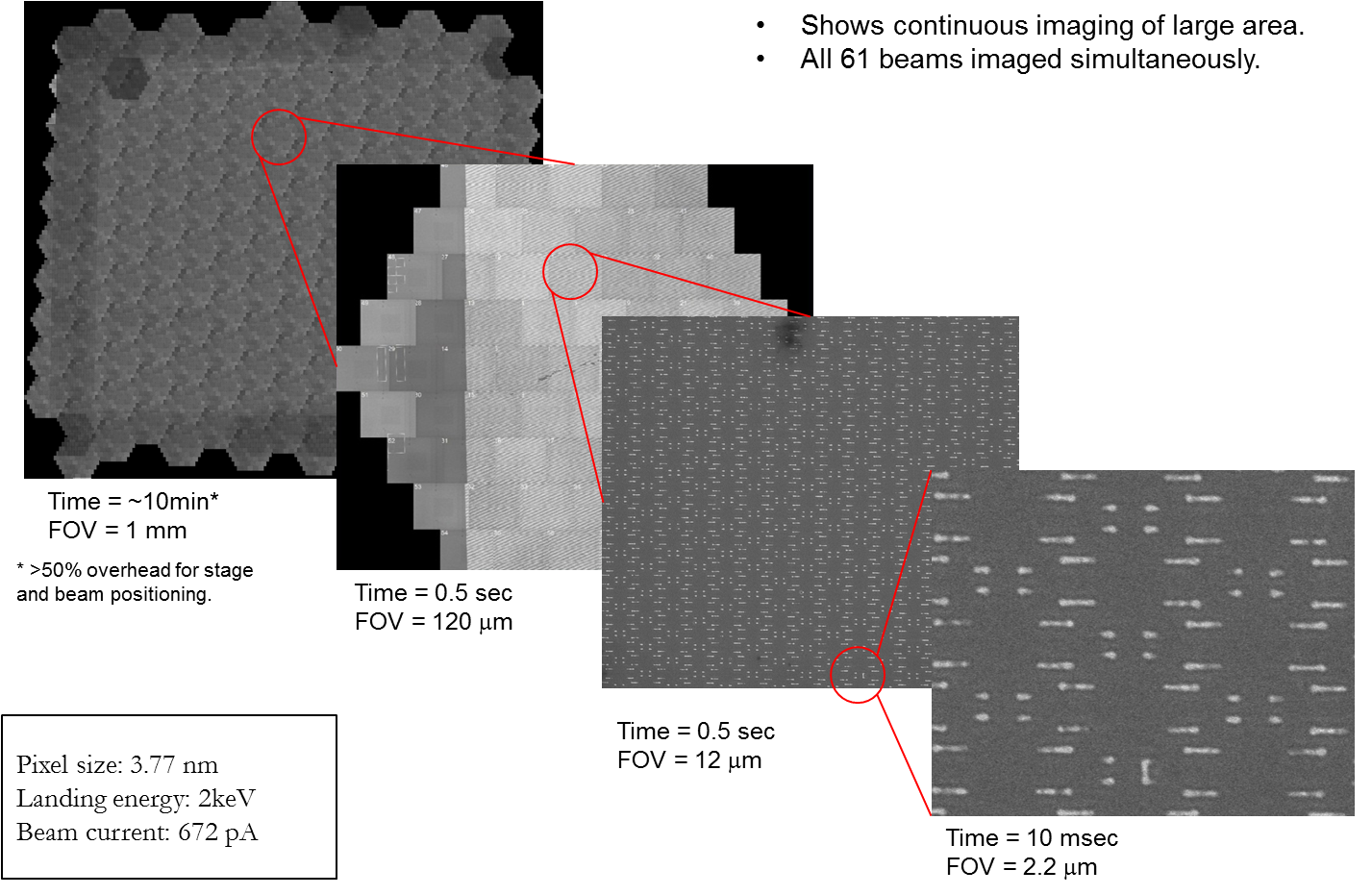
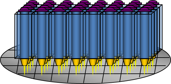
Electron beam technologies are both powerful and versatile for a wide range of nanotechnology applications. Their chief drawback, however, is speed for macroscopic applications. Inspecting an entire 300 mm silicon wafer for patterning defects in microelectronics manufacturing would take several months under typical conditions. Creating macroscopic structures using single beam EBID is even slower. One solution is the use of massively parallel arrays of electron beams working in unison. One means of producing a large array of beams is by splitting a single beam into many beamlets within a single electron-optical column. An alternative approach involves making large arrays of miniature columns. Both approaches have advantages and disadvantages depending on the specific application, but all applications and implementations depend on achieving a high degree of uniformity in the behavior of the beamlets in the
array. Our work in this area is in determining the relevant performance specifications needed for various applications as well as devising methodologies for assessing the variations. A specific example is the use of contrast transfer functions to determine the sensitivity to semiconductor patterning defects as a function of SEM operating parameters.